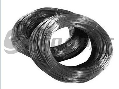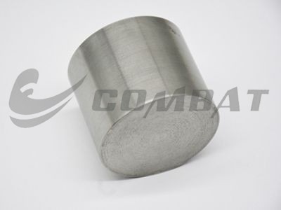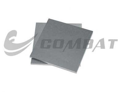


Molybdenum Sputtering Target for Semiconductor Manufacturing
作者:kangbote 时间:2026-10-20 15:36:08
The purity, microstructure, density and dimensional consistency of PVD sputtering targets directly affect plasma stability, particle emission and film uniformity. The molybdenum target with insufficient purity and uneven grain size will make the re-optimized sputtering formula unable to reproduce. This article explains the working principle, material advantages, key specifications, manufacturing process and selection methods of molybdenum sputtering targets in semiconductor manufacturing, and helps the process and procurement team to establish a complete judgment framework from target arrival to film yield.
What Is Molybdenum Sputtering Target?
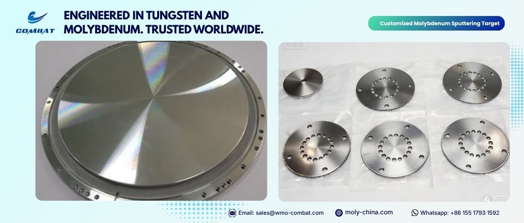
A molybdenum sputtering target is a solid piece of high purity molybdenum metal or molybdenum alloy as a source material for sputtering processes in physical vapor deposition (PVD). In the vacuum chamber, high-energy ions bombard the target surface, and the molybdenum atoms are ejected layer by layer onto the silicon wafer, glass or flexible substrate to form a continuous film.
According to the geometry is divided into two categories: flat target (disc, square plate, rectangular) and rotating tubular target. Planar targets are used in R & D lines and most semiconductor equipment. The rotating target achieves more uniform erosion through uniform rotation, and the material utilization rate can reach 70%-80%, mainly serving panels and large-area glass production lines.
How Does A Molybdenum Sputtering Target Work?
Molybdenum is a conductive metal, and almost all of the industry uses DC magnetron sputtering. The whole process can be broken down into six phases.
1.The vacuum chamber draws a background vacuum. The molybdenum target is installed in the vacuum chamber as the cathode, facing the substrate. The chamber is pumped to the order of 10 rex Torr to remove residual gas contamination, and then filled with low-pressure argon (a few mTorr) as the working gas.
2.Glow to form plasma. A DC voltage of several hundred volts is applied between the cathode and the anode, and the free electrons hit the argon atoms to ionize them into Ar + ions and more electrons, forming a glow discharge.
3.The magnetic field confines the electrons. The permanent magnet on the back of the target builds an orthogonal electromagnetic field, which constrains the electrons to move near the target surface, greatly increases the plasma density, and obtains a higher deposition rate than ordinary two-pole sputtering.
4.Ion bombardment and atom escape. The positively charged argon ions bombard the surface of the molybdenum target under the acceleration of the electric field, and by virtue of the kinetic energy of tens to hundreds of eV, the molybdenum atoms are separated from the surface of the target and enter the gas phase through the collision cascade effect.
5.Transport and film formation. Molybdenum atoms produced by sputtering migrate in a straight line in a vacuum environment and deposit on the surface of the substrate to form a continuous film.
6.Target erosion and life. Flat molybdenum targets will form racetrack-shaped erosion grooves; rotating tubular targets rely on rotation to achieve uniform wear. When the target erosion reaches its limit, it needs to be replaced.
Why Is Molybdenum Used In Semiconductor Thin Films?
The fact that molybdenum can stand simultaneously in the gate, barrier and interconnect 3 a scenario is rooted in the physical and chemical parameters of the 1 groups that cooperate with each other, rather than a single indicator.
High melting point stability
Molybdenum has a melting point of about 2617-2623°C and a thermal conductivity of 138-139 W/m · K. This set of data means two things: 1, the target surface does not melt and does not produce thermal warpage under high power density; 2, the film layer does not soften and volatilize in high temperature steps of 400-600°C such as CIGS selenization and gate annealing.
Low resistivity
The resistivity of the molybdenum block is about 5.2? Ω-cm, and the optimized film can achieve 10-20? Ω-cm. More importantly, molybdenum has a short mean free path for electrons, and its resistance advantage exceeds that of copper and tungsten at ultra-thin film thicknesses (below 7-8 nm)-which is exactly what advanced node contact holes, word lines and hybrid metallization require.
Coefficient of thermal expansion
Molybdenum has a coefficient of thermal expansion of about 4.8 × 10+6/K, which is among the lowest 1 among commercial metals. The CTE of glass, silicon wafer and ceramic is close to these 1 values, the residual stress of the film in the thermal cycle is small, and the risk of cracking and delamination is significantly reduced.
Electromigration resistance and chemical inertness
The molybdenum film has a long electromigration life at high current density and can block the diffusion of copper or aluminum atoms into the dielectric layer and silicon in the multi-layer stack. In CIGS solar cells, the molybdenum back contact layer also reacts with selenium to form a layer of MoSe₂, which instead forms a favorable ohmic contact interface.
Process compatibility with DC magnetron sputtering
The conductive target is directly driven by a DC power supply and does not require RF matching or intermediate frequency pulses. This allows the molybdenum sputtering target to have a process cost advantage in large-area uniform coating and high-energy production lines.
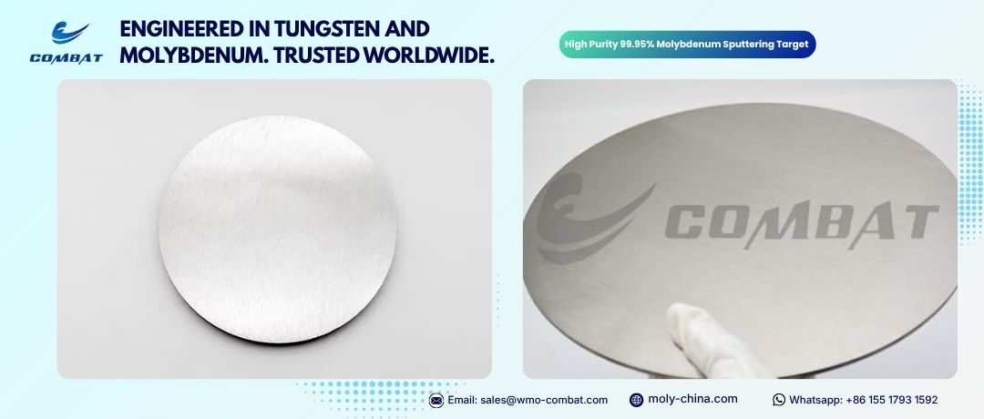
Application of Molybdenum Sputtering Target in Semiconductor
Interconnect Barrier and Adhesion Layers
In the back-end interconnect structure, a 5-20 nm thick molybdenum film is sandwiched between the copper interconnect and the low-k dielectric. It prevents the diffusion of copper atoms to silicon and dielectric in the long-time annealing at 400°C, while improving the adhesion of the copper seed layer to the underlying material. In addition to pure molybdenum, alloy targets such as Mo-Ti, Mo-Nb, and Mo-Ta are used for multi-layer stacking, and the anti-diffusion performance is more robust under the BEOL thermal budget.
Gate, Source and Drain and Contact Metallization
Molybdenum has a work function of about 4.6 eV and is suitable for gate electrodes of MOSFETs and TFTs. It has a stable resistance at a high temperature step of 600°C, and its contact resistance with silicon or oxide semiconductor is controllable.
The source and drain terminals are usually stacked with Mo/Al/Mo or Cu/MoTi: the upper and lower layers of molybdenum are responsible for adhesion and blocking, and the middle aluminum or copper is responsible for low resistivity. In the IGZO oxide TFT, the MoTi alloy target is specifically used to block the diffusion of copper into the oxide active layer.
Display Panel and Semiconductor Thin Film Technology
TFT-LCD and OLED backplanes are one of the largest application scenarios for molybdenum sputtering targets. Molybdenum or molybdenum alloys (Mo-Nb, Mo-Ta, MoW) are widely used for the gate, source and drain electrodes of the a-Si, LTPS, and IGZO three-type TFTs because of good etching selection ratio and resistance to subsequent process temperatures.
In the broader field of microelectronics, molybdenum films also appear in Mo/Si multilayer Bragg mirrors for SAW/BAW filters, MEMS devices, and EUV mask blanks.
Specifications of Semiconductor Grade Molybdenum Target
The molybdenum target specification determines the defect rate of the film layer. When purchasing molybdenum sputtering targets, semiconductor customers must focus on at least four dimensions: chemical purity, density, grain size, and thermal mechanical size.
Chemical Purity and Impurity Control
The tolerance for purity varies widely from application to application. The following table divides the selection interval according to the common grade:
|
Purity grade |
Typical Purity |
Applicable Scenarios |
Key impurity control |
|
3N |
99.9 percent |
Decorative coating, non-critical R & D samples |
Metal impurities 100 ppm acceptable |
|
3N5 |
99.95 percent |
TFT-LCD, CIGS, General Semiconductor Barrier |
Single elements such as Fe/Ni/Cu <10-20 ppm |
|
3N7-4N |
99.97-99.99 percent |
Advanced Logic/Storage Node Gates and Contacts |
Oxygen <40 ppm, single digit ppm of metallic impurities |
|
4N5 |
99.995 percent |
The most advanced node, EUV related multilayer film |
GDMS full spectrum scanning, strict control of gap elements |
Oxygen content is the most underestimated indicator. Excessive oxygen will directly raise the film resistivity and increase particle emissions. Advanced high purity molybdenum targets require oxygen to be controlled within 40 ppm or even lower. Interstitial elements such as carbon and nitrogen should also be minimized.
Density and porosity
The theoretical density of molybdenum is about 10.2g/cm3. The actual density of high-quality sputtering targets should reach more than 99.5 of the theoretical value, I .e. the range of 10.15-10.22g/cm³. Residual porosity is one of the main sources of particles. The pores break up under ion bombardment, and the sputtered micron-sized particles fall directly onto the substrate to cause defects. High density targets simultaneously improve heat conduction, allowing higher power density operation.
Grain Size and Microstructure Uniformity
The average grain size of semiconductor grade molybdenum sputtering targets is usually required to be controlled below 100 µm, and high-end HIP (hot isostatic pressing) materials can achieve 10-50 µm. Coarse or uneven distribution of grains will lead to preferential erosion of the target surface, runway drift and increase in the number of particles. The grain size in the thickness direction of the whole plate should be uniform to avoid banded structure or gradient. Metallographic sections are rated according to ASTM E112 as a routine means of acceptance.
Electrical, thermal and dimensional parameters
The following table summarizes the 1 set of benchmark data commonly used in semiconductor procurement:
|
Parameters |
Typical value/description |
|
volume resistivity |
Approximately 5.2 µΩ · cm(0°C bulk value) |
|
Melting Point |
2617-2623°C |
|
Thermal conductivity |
138-139 W/m·K |
|
Coefficient of thermal expansion |
about 4.8 × 10 over/K |
|
theoretical density |
Approximately 10.2g/cm³ |
|
Quartz crystal monitoring Z factor |
Approximately 0.257. |
|
Upper limit of unbonded target power density |
Approximately 150W/in² (reference value, subject to plant specification) |
High power processes typically bond a molybdenum target to a copper backing plate using indium or elastomer. The bonding target is a protective layer, and the power density should be reduced to about 20W/in². Bonding coverage is recommended 95%-98%, and ultrasonic scanning is used to detect voids.
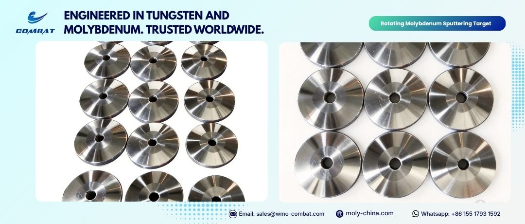
How Is The Molybdenum Sputtering Target Made?
The semiconductor grade molybdenum target takes the powder metallurgy route, and the core goal is to achieve the 3 indicators of high purity, high density and fine grain at the same time.
Preparation of high purity molybdenum powder
The raw material starts from molybdenite (MoS₂): flotation enrichment → oxidation roasting to MoOover → multi-stage hydrogen reduction to obtain pure molybdenum powder. The temperature and atmosphere curve of multi-stage reduction directly determine the residual oxygen content, and the oxygen pressure is reduced to tens of ppm in industry. The alloy target (Mo-Nb, Mo-Ti, etc.) is fully mixed with the alloy element powder and molybdenum powder in an inert atmosphere to ensure uniform composition.
Consolidation and microstructure control
The powder is first subjected to cold isostatic pressing (CIP) or compression molding to obtain a green compact with a density of about 50% to 65%.
The green body is sintered at high temperature (about 1800-2100°C) in hydrogen or vacuum, and the density is increased to 90%-97%, while further deoxidation.
Subsequent hot isostatic pressing (HIP) treatment at 1100-1600°C and 100-200 MPa pressure closes the residual pores and pushes the relative density to 99.5-99.9%.
Sintering and HIP are usually followed by hot rolling, forging or extrusion. Thermomechanical crushing breaks the coarse grains and presses the grain size below 100 µm. Intermediate annealing controls recrystallization and residual stress.
Precision Machining and Bonding
The compact blank is milled, ground and turned to final geometric dimensions by CNC. Grind or polish the sputter face to Ra ≤ 0.8 µm and chamfer the edges as required. The high power molybdenum target is then indium soldered or elastomer bonded to the copper backing plate. The bonding interface must be free of voids, otherwise the local thermal resistance increase will cause the target surface to crack.
Factory inspection and traceability
Semiconductor grade molybdenum sputtering targets require full batch traceability, complete archiving from molybdenum powder batch number to machining records.
How To Choose Right Molybdenum Target For Semiconductor Manufacturing?
The selection is not to choose the "highest specification", but to match the molybdenum target grade with the process window, to avoid excessive specifications to push up costs, but also to avoid the loss of yield caused by insufficient specifications.
Step 1: Select application and process conditions
Gate/barrier layers for advanced storage or logic nodes → highest purity (4N +), finest grain size.
TFT-LCD/OLED panel electrode → 3N5 purity, large area uniformity priority, rotating target more economical.
CIGS back contact → thermal stability and CTE matching with soda lime glass are preferred.
At the same time, the equipment parameters are recorded: plane cathode or rotating cathode, power density range, substrate temperature, target base distance, target target material life. These parameters directly determine whether the backplane needs to be bonded and how much power is allowed.
Step 2: Match purity, density and grain size
Translate the film requirements into molybdenum target indicators: the lower the target sheet resistance, the stricter the particle limit, the higher the purity and grain size requirements. The density shall not be less than 99.5% of the theoretical value. Grain size advanced process requirements ≤ 100 µm, higher requirements ≤ 50 µm.
Step 3: Geometry and Bonding Scheme
The core differences between a flat target and a rotating sputtering target are as follows:
|
Contrast Item |
flat molybdenum target |
rotating molybdenum target |
|
erosion morphology |
Fixed "runway" groove, material utilization rate of about 30%-40% |
Uniform wear throughout the week, the utilization rate can reach 70%-80% |
|
Typical Scene |
Research and development line, semiconductor monolithic equipment, small batch production. |
Panel Gen line, large area glass, high production capacity roll-to-roll |
|
Equipment Requirements |
Universal planar magnetron cathode, wide compatibility |
Special rotary cathode and rotary seal feed required |
|
Cost structure |
The price of a single piece is low, but the replacement is frequent and the comprehensive utilization rate is low. |
High initial investment, better long-term monolithic cost and replacement downtime |
Step 4: Evaluate Sputtering Target Supplier's Manufacturing Consistency
What really distinguishes the supplier level of molybdenum metal materials is not the single point parameter, but the batch-to-batch consistency. Examine several hard indicators:
- Whether it has its own powder metallurgy molybdenum material manufacturing full link, rather than the simple outsourcing processing of purchased blanks.
- The process control curve of oxygen content and grain size can provide continuous multi-batch statistical data.
- Whether there is an internal laboratory for ultrasonic scanning, GDMS and metallographic sample preparation, or whether all of them are sent out for testing.
- Can new suppliers supply sample targets for coating verification before batch supply.
Whether the packaging is vacuum clean packaging in a controlled environment, and no secondary pollution is introduced during transportation.
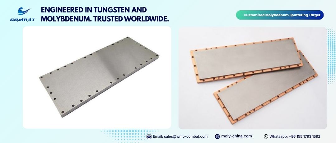
Frequently Asked Questions about Molybdenum Sputtering Targets
Q1: What does molybdenum sputtering target mainly do in semiconductor manufacturing?
There are three main types of roles: diffusion barriers and adhesion layers for copper/aluminum interconnects, MOSFET/TFT gate electrodes and source/drain contacts, and hybrid metallization layers in advanced memory and logic.
Q2: Semiconductor grade molybdenum target need more high purity?
3N5(99.95%) is enough for panels and CIGS; Advanced logic and storage nodes are recommended to start at 99.97-99.99% and key layers at 99.995%(4N5). The oxygen content is generally required to be <40-100 ppm.
Q3: Why does grain size affect target performance so much?
Coarse grain or uneven grain size will make the target surface preferentially eroded at the grain boundary, the runway shape drifts, the film thickness uniformity deteriorates, and the number of particles increases. Fine grain (≤ 100 µm) ensures uniform erosion, stable sputtering rate and low particle emission.
Q4: What is the melting temperature of molybdenum target?
2617-2623°C. This high melting point allows the molybdenum target to withstand high power density without melting the target, which is the basic condition for DC magnetron sputtering.
Q5: Molybdenum target can be customized size?
Yes. The diameter of the sputtering target, the length, width and thickness of the rectangular plate, the diameter, length and wall thickness of the rotating target, as well as the purity grade, grain size, bonding method and installation interface can be customized according to the equipment drawings. Research and development of small quantities and mass production of large quantities can be undertaken.
Conclusion
The molybdenum sputtering target is not a standard part purchase item, but is part of the PVD process window. Target purity determines film resistivity and defect baseline, grain size determines particle emissions and runway life, and density and bonding determine the upper power limit that can be tolerated.
Combat is a focus on refractory metal (molybdenum, tungsten, tantalum, titanium) and alloy target manufacturers, with a complete metal sputtering target production line. The purity of semiconductor grade molybdenum target can reach 99.95%, and it supports a full range of customization of flat and rotating targets.
If you are evaluating a molybdenum target supplier for a semiconductor manufacturing line, you are welcome to send the target drawing, target purity level, equipment model and power density requirements, and our engineering team will feedback the matching plan within two working days.